


Adam McCaughan
Physicist, National Institute of Standards and Technology
Education
- Ph.D. (2015) • Electrical Engineering Massachusetts Institute of Technology
- M.Eng. (2010) • Electrical Engineering • Massachusetts Institute of Technology
- B.S. (2009) • Electrical Engineering • Massachusetts Institute of Technology
Current Position
- Physicist, National Institute of Standards and Technology, Applied Physics Division, Boulder, CO
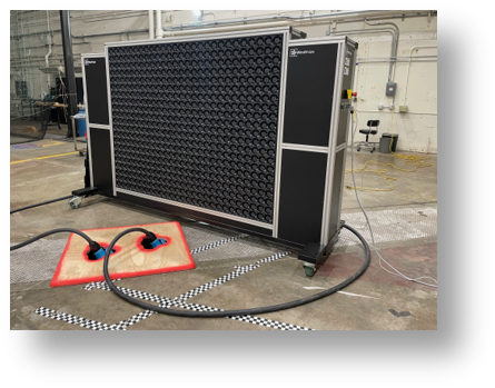
- Developing superconducting nanowire single-photon detectors in the ultraviolet, designing architectures for megapixel-scale array.
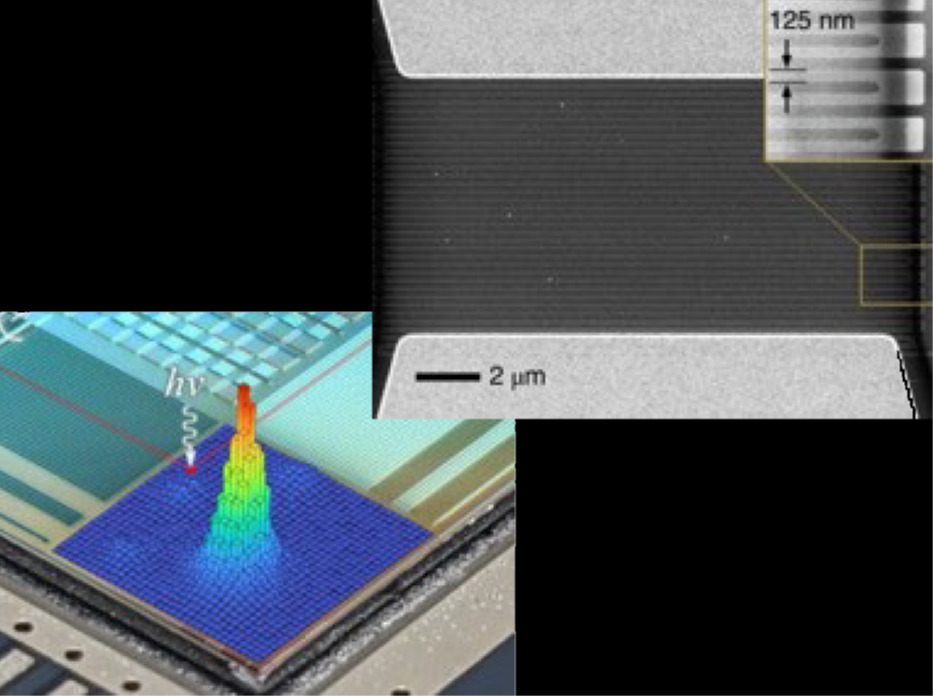
Bottom left: a microscope picture of a silicon chip. Overlaid is a 3D histogram representing the arrival of photons in a gaussian-distributed area at the center of the camera. Upper right: a scanning electron micrograph showing a zoomed image of a nanowire structure.
Technology Interests
- Superconducting nanowire single photon detectors
- Electrothermal nanowire electronics for amplification and readout of superconducting signals
- Vertically aligned carbon nanotubes
- Machine learning and optimization frameworks
Goals and Aspirations
- Creation of a multi-megapixel single photon detector array that has near-unity efficiency and fill factor
- Integrating carbon-nanotube absorbers with SNSPDS to create broadband single-photon detectors.
- Increasing the operating temperature of SNSPDs to ease space flight requirements
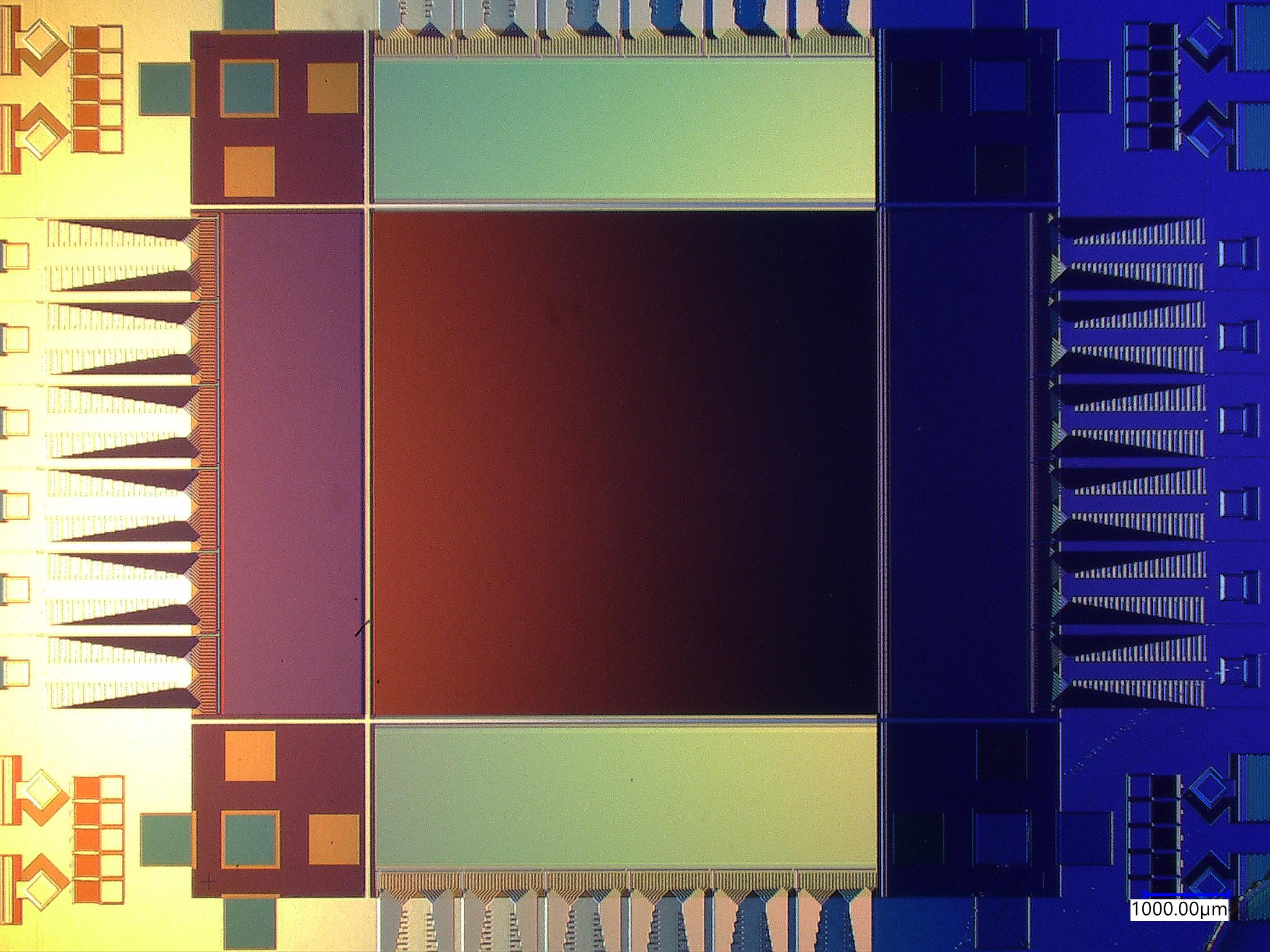
A microscope image of a rectangular chip, showing the different parts of the superconducting camera, including imaging area and ancillary electronics.