PROJECT
Development of a Robust, Efficient Process to Produce Scalable, Superconducting Kilopixel Far-IR Detector Arrays
SNAPSHOT
An SMD-sponsored team has taken major steps towards providing the new detector arrays needed for future far-infrared space missions.
In the Decadal Survey on Astronomy and Astrophysics 2020, the National Academy of Sciences recommended to NASA a series of competed probe-class missions, including one with far-infrared (FIR) imaging or spectroscopy capabilities. The Academy also recommended that technology development for a future flagship-class FIR mission commence. Both types of missions would require cryogenic telescopes with unprecedented sensitivities and mapping speeds to enable FIR science.
Telescopes with these capabilities would allow the astronomical community to address a wide range of scientific objectives such as measuring the masses of protoplanetary disks; tracking the role of water, ice, and volatiles in planet formation; and investigating the interplay between the interstellar medium and star formation across the Milky Way. A cryogenic FIR observatory would also allow scientists to diagnose the state of gas and its radiation environment in nearby galaxies, including outer galaxy disks and extra-planar material associated with feedback and gas accretion.
In addition, observations made with these advanced telescopes would allow scientists to study the evolution of galaxies and the matter they are made of throughout the history of the universe—from the formation of the first dust clouds, to star-forming galaxies at the cosmic noon (a time when significantly more stars per time unit were formed than today). Such studies could also include detailed investigations of the matter that our own galaxy, the Milky Way, is made of.
Observing light at the wavelengths invisible to our eyes, these observatories will be able to see through the layers of matter that block the light in the visible part of the electromagnetic spectrum. Even regions where foreground matter completely blocks the view (like the bricks of a house that will not let see you what is inside) will be visible in the far-infrared. These new telescopes will be able to observe massive black holes that are embedded in the dense central regions of many galaxies. Such observations will allow astronomers to determine how the creation of black holes proceeded throughout the history of the universe.
To make these types of observations, NASA’s future telescopes need robust, high-sensitivity, kilopixel-format arrays that operate over the entire far-IR spectrum. Previously, some of the key technologies needed for these arrays were demonstrated on the High-resolution Airborne Wideband Camera (HAWC+) on the Stratospheric Observatory for Far-Infrared Astronomy (SOFIA). Those detectors provided excellent performance for suborbital far-IR applications, but their production was very labor intensive with relatively low fabrication yields. The remaining major technologies required to enable future FIR space-based telescopes are: (a) robust detector array architectures with approximately 100,000 individual pixels and (b) integrated readout multiplexers that can meet the ultra-low noise requirements of space missions.
The NASA Astrophysics Division’s Strategic Astrophysics Technology (SAT) Program is sponsoring a team from NASA's Goddard Space Flight Center (GSFC) in Greenbelt, Maryland, and the National Institute of Standards and Technology (NIST) in Boulder, Colorado to address this need. Led by Dr. Johannes Staguhn at the Johns Hopkins University/GSFC, the team is maturing and streamlining the processing required to produce arrays with large numbers of pixels (10,000) that can be tiled to deliver the desired 100,000 pixel count.
The project will advance the technology to Technical Readiness Level 5 (defined as component and/or breadboard validation in a relevant environment), an important step towards maturation of technologies for eventual space flight.
Enabling a Kilopixel Detector Array
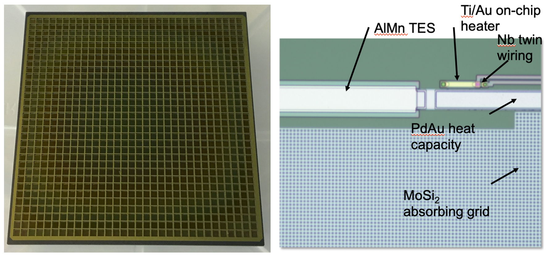
The team has successfully produced all the individual components required for the new detectors. First, the team developed detector wafers that could be bonded together to produce a detector with the required 100,000 pixels. The figure below shows a picture of the detector wafer (left image), which consists of 1024 individual pixels. The image on the right shows a zoomed-in view of part of an individual pixel. Each pixel contains one superconducting detector, which is a Transition Edge Sensor (TES) made from aluminum manganese (AlMn). Part of the absorber mesh, which is tuned to the electromagnetic radiation coming from the telescope, can also be seen in the righthand image.
Detector Hybridization: Integrating the Detector Arrays with a Readout Board
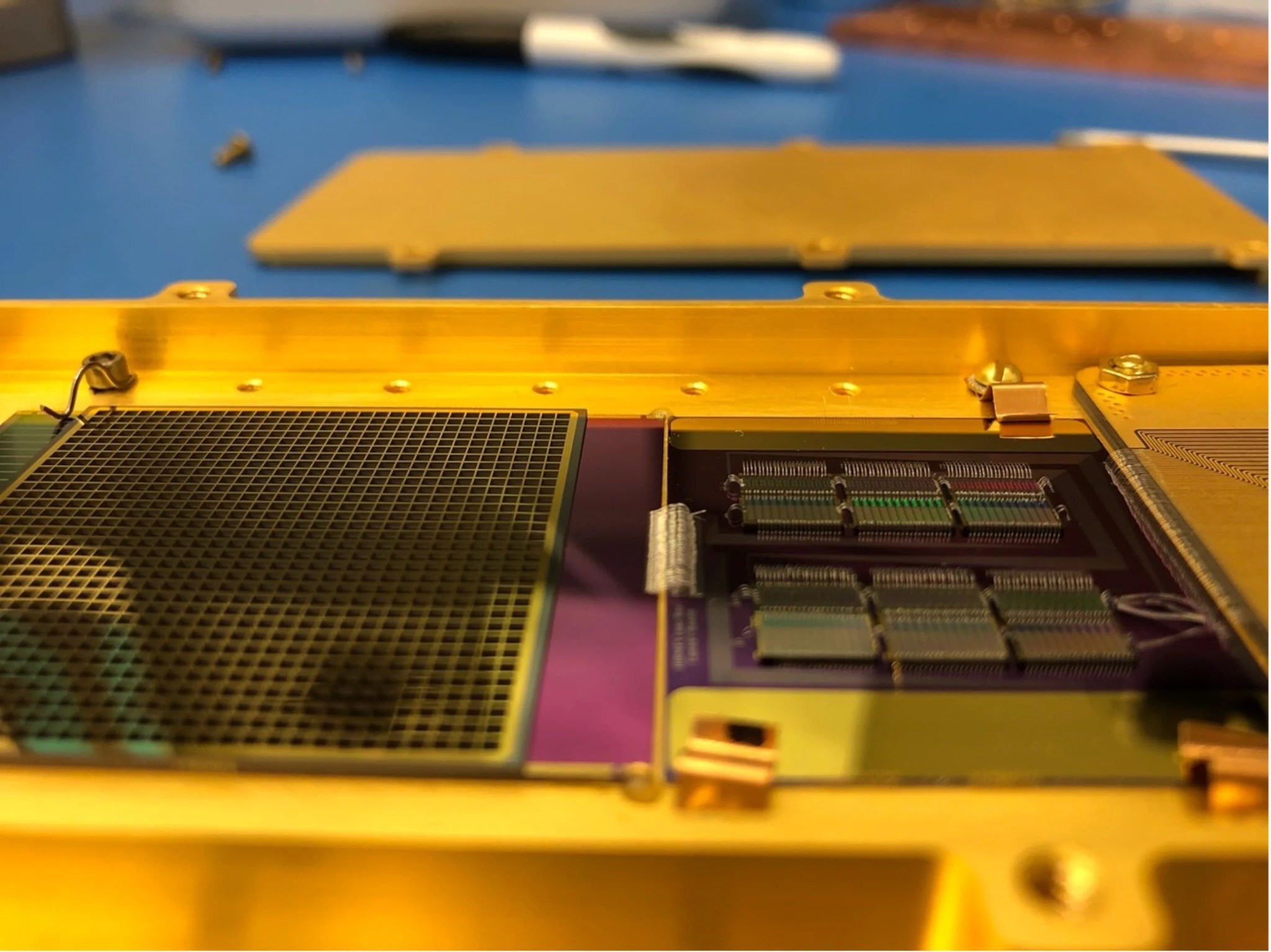
Developing a kilopixel detector required the team to use a process called “hybridization,” that allows the detector wafers to be bonded together. Indium “bumps” are deposited on dedicated landing spots on each of the wafers, and then the wafers are pushed together. The bumps on one wafer stick to those on the other, resulting in a superconducting connection between the wafers. Using this method, the team recently completed development of the first kilopixel detector, which consists of a hybridized “Double Stack” detector, a readout board, and 64 channels of ultra-sensitive Superconducting Quantum Interference Devices (SQUIDs) (see image below).
Testing of this detector is underway, and so far, all measured device parameters (e.g., the thermal conductivity, saturation power, and transition temperature) are consistent with expectations.
The Final Product: A “Triple Stack” Detector Array
The end product of this project was the demonstration of a fully bump-bonded “Triple Stack” detector array (shown in the image below). A so-called “interposer board” was bump-bonded to the detector array. This “double stack” then was successfully bump-bonded to a fanout board. The resulting triple stack, mounted in a readout package, is shown below. Using this new detector, the team was able to successfully measure several devices that were wired up for readout, marking the first time that a double layer of superconducting indium bump bonds was successfully demonstrated.
Conclusion
“We are very pleased with the results we see,” says Dr. Staguhn. “With the exciting far-infrared roadmap that the Astrophysics Decadal Report has laid out for the community, we are in urgent need of efficient and reliable superconducting detector arrays that can meet the very challenging requirements of upcoming space missions such as a far-infrared probe. The detector architecture we have demonstrated here is an important stepping stone towards those goals”.
PROJECT LEAD
Dr. Johannes Staguhn, GSFC/Johns Hopkins University
SPONSORING ORGANIZATION
Astrophysics Division Strategic Astrophysics Technology (SAT) Program

