


This blog post originated in the 2018 Science Mission Directorate Science and Technology Report.
PROJECT
Nanoscale vacuum channel transistor (NVCT)
KEY POINTS
To help protect future space assets from dangerous effects that arise from radiation exposure, NASA is developing a new series of vacuum electronics that are ultra-small, easy to manufacture, and immune to radiation damage.
All space missions face a high risk of radiation-induced damage to electronics. Unfortunately, the current strategies employed to limit radiation exposure all introduce various mission constraints. NASA is exploring use of an “old school” technology—vacuum electronics—combined with modern techniques to protect the Agency’s important space assets without restricting mission parameters.
NASA implements various strategies to avoid radiation impacts to missions including: (1) limiting the flight and exploration path to minimize radiation exposure, (2) use of radiation shielding based on a metal chassis, and (3) incorporating chip designs with radiation awareness. However, all of these tactics introduce mission constraints. Limiting the exploration path leads to delays and constrains the exploration area. Furthermore, it is intrinsically impossible to avoid unexpected radiation exposure. The metal radiation shield adds significant weight, impacting the launch cost. A radiation-aware design is expensive and limits the available hardware options because not all the required parts can be found in space-grade pool of available equipment. Another serious emerging problem is the dwindling number of U.S. companies supplying radiation-hardened electronics due to the low-volume nature of the business.
Vacuum devices of the early electronics era were immune to space radiation but they were bulky and energy-hungry. More importantly, they were not amenable to large-scale manufacturing, as we know today. Silicon-based integrated circuits successfully demonstrated their potential to overcome the shortcomings of the vacuum devices, ushering in the modern electronics revolution and sunsetting the vacuum electronics era. Except, all modern electronics devices using silicon, gallium arsenide, andother materials are vulnerable to radiation, posing challenges to space mission designers to come up with ways to mitigate the radiation impact. It is not uncommon for missions to incorporate electronics technologies several generations behind the state-of-the-art due to the time-consuming process associated with finding the right solution to protect the electronics from the deleterious effects of space radiation.
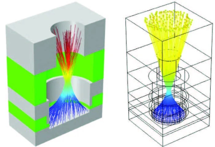
A team at NASA Ames is developing the nanoscale vacuum channel transistor (NVCT) by combining the best of vacuum electronics—known for radiation immunity—with modern integrated circuit manufacturing practices that excel in making ultra-small devices. In a nutshell, the semiconductor channel in a transistor is replaced with an empty gap in the NVCT. Unlike the channels in a semiconductor, which suffer from lattice scattering, this vacuum channel enables ultra-high electron velocities in the NVCT. NVCTs can be fabricated using any of the common semiconductor materials such as silicon, gallium arsenide, silicon carbide and others.
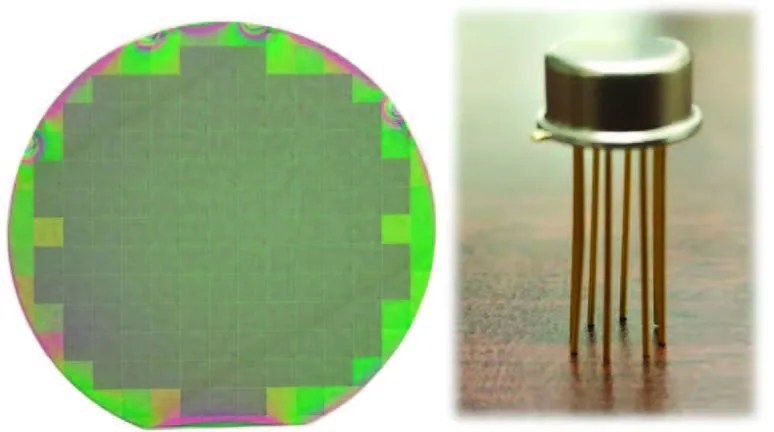
In the last 18 months, the Ames team has successfully fabricated silicon as well as silicon carbide NVCTs on 150-200-mm wafers with dimensions comparable to conventional metal-oxide semiconductor field-effect transistors (MOSFETs). The smallest silicon NVCT has a 50-nm source-drain distance with a surround gate. To make the NVCT drive currents comparable to conventional MOSFET devices, multiple emitter tips are needed. For this reason, the team chose a vertical configuration for the NVCT with the source pad hosting multiple emitter tips at the bottom, a common collector at the top, and a gate wrapping around the channel for ideal electrostatic control. The NVCT device current was shown to scale linearly with the number of emitter tips, offering design flexibility for achieving desired mA current levels. Unoptimized initial NVCT devices show a potential of 0.5 THz operation. Exposure to radiations at doses typically experienced by space missions (a few tens of MRad gamma radiation and 10 MeV fast neutrons) showed negligible impact on device characteristics.
These successful results at the transistor level are encouraging, and now the NASA team is developing circuit-level vacuum devices. The current effort involves adding on-chip resistors and capacitors to the wafers hosting the NVCTs to facilitate assembly of functional circuits. The next planned step will demonstrate a working “flip-flop” circuit and assess the radiation impact on that circuit.
Radiation-immune nanoscale vacuum electronics will be highly valuable to many NASA missions, including exploration missions to Europa, which will face extreme radiation environments and low temperatures. Measures similar to the Juno Radiation Vault—a titanium compartment that protects the electronics on the Juno spacecraft—may be needed to protect vulnerable electronics in these missions. Such measures increase weight and mission complexity and do not entirely ensure radiation immunity. Electronics failure could lead to mission failure, thus the NVCT effort could have a significant impact on future missions by eliminating the need for such vaults.
SPONSORING ORGANIZATIONS
Planetary Science Division’s Icy Satellites Program
PROJECT LEAD
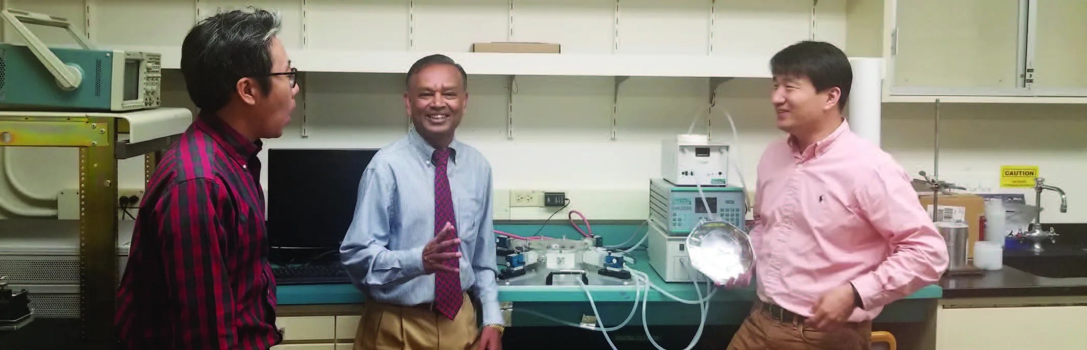
Dr. Meyya Meyyappan, NASA Ames Research Center
Read more Technology Highlights