


PROJECT
Advanced FUV/UV/Visible Photon Counting and Ultralow Noise Detectors
SNAPSHOT
Researchers have developed methods to alter the surface properties of ultraviolet detectors and produce instruments with unprecedented sensitivity and performance.
The ultraviolet (UV) spectral range is rich with information about the atmospheres of exosolar planets, star formation, supernovae, the circumgalactic medium, and much more. Two future flagship mission concepts, Habitable Exoplanet characterization (HabEx) and Large Ultraviolet/Optical/Infrared survey mission (LUVOIR), would cover the important UV region. These powerful Earth-orbiting telescopes need detectors that are efficient, sensitive, and optimized for this specific spectral range; otherwise, the majority of photons these telescopes intend to gather will remain “unseen.” A NASA JPL team has developed new detector technologies that will enable instruments on these and other NASA missions.
Seeing the Unseen
"Everyone sees the unseen in proportion to the clarity of his heart, and that depends upon how much he has polished it. Whoever has polished it more sees more - more unseen forms become manifest to him."
—Rumi, Persian Poet and Mystique 1207 – 1273
The challenge involved in detecting ultraviolet photons is almost universally experienced by anyone who has suffered a sunburn. Because ultraviolet light is absorbed in the first few nanometers of most materials, our skin suffers the damaging effects of ultraviolet radiation rather than our internal organs. In semiconductors and specifically silicon, UV absorption also occurs within the first few atomic layers of the surface, where defects can trap electrons and prevent detection. Unless these defects are passivated, the UV signal will remain unseen or undetected.
A NASA JPL team has developed new ways to refine the surfaces of UV detectors using two techniques—2D-doping (intentionally introducing impurities to change surface properties) and atomic layer deposition (ALD) to filter the light and tailor the detector response. Applying these surface engineering technologies to detectors capable of single photon sensitivity leads to reliable, repeatable, and unprecedented UV performance.
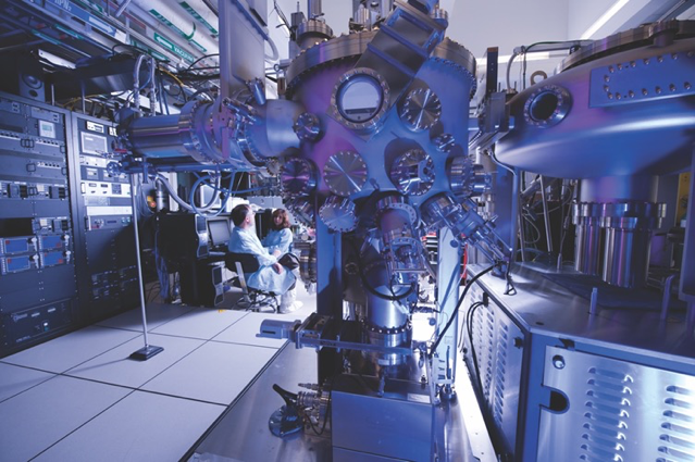
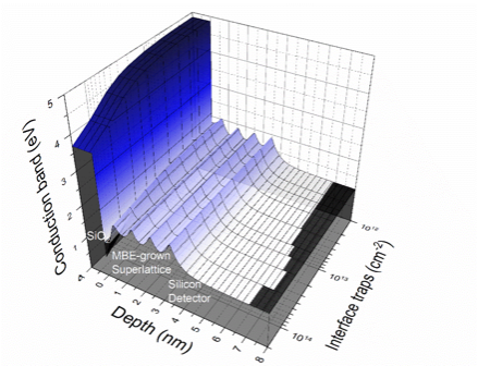
Atomically precise control of surfaces and interfaces is essential to improving the performance of various devices. This nanoscale tailoring is particularly important for detectors in the UV spectral range, where photons are absorbed in the first few nanometers of the silicon surface. Precise engineering of detector surfaces using molecular beam epitaxy (MBE) allows UV-produced electrons that would otherwise be trapped in the silicon to be detected. The energy bands that result from the atomic-scale crafting of the surfaces are shown below. Using 2D-doping, detectors are enabled to “see” every photon that is absorbed in the silicon surface.
Optimizing the selectivity and degree to which photons are absorbed or rejected requires further surface and interface engineering. The NASA JPL group used atomic layer deposition (ALD) for this purpose. ALD is a thin-film deposition technique based on sequential, self-limiting, chemical reactions. Chemical reactants are introduced to the substrate in separate steps isolated by purges with a non-reactive gas, as depicted in the simple schematic below.
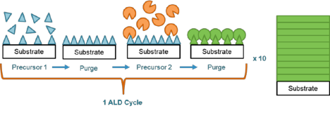
ALD enables precise deposition of ultrathin films with sharp surfaces and interfaces and is ideal for coating detectors with multilayer dielectrics or multilayer metal-dielectrics that are designed to enhance wanted light and filter out unwanted light. Metal layers are needed that can block visible light but transmit UV light into the detector. Aluminum can be transparent, as Mr. Scott famously illustrates in a scene from Star Trek IV: The Voyage Home (Onlooker: “Transparent aluminum!?” Mr. Scott: “That’s the ticket laddie!”) and fortunately, aluminum is transparent in UV. The NASA-JPL group fine-tuned the detector’s UV response by alternating multilayer dielectric films with layers of aluminum, which transmit UV light but block visible photons.
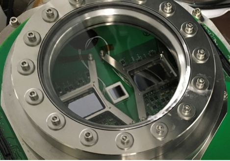
Photon counting (or single photon sensitivity) can be realized in solid state detectors by internally amplifying the signal, e.g., in electron multiplying charge-coupled devices (EMCCDs). Because 2D doping and integrated filter technologies are versatile and applicable to a variety of silicon detector architectures, it is possible to apply them to the latest cutting-edge silicon detector designs, including EMCCDs as well as other devices with gain and low noise. High-efficiency 2D-doped and tailor-coated EMCCDs have been demonstrated and deployed in suborbital missions, as described below. In other instruments such as those baselined for LUVOIR, 2D-doped and ALD-tailored complementary metal oxide semiconductor (CMOS) detectors could potentially be used.
The predecessors to this advanced technology can be found in everyday life; cameras on cell phones typically employ silicon imagers—especially CMOS detectors—to generate images in the visible spectrum. Given the ubiquity of these devices, this current technology development effort is quite remarkable. First, it effectively leverages the previous and current investments in silicon imaging. In addition, this effort has converted a technology designed to enable photography into one that produces highly efficient UV imagers that are blind to visible light.
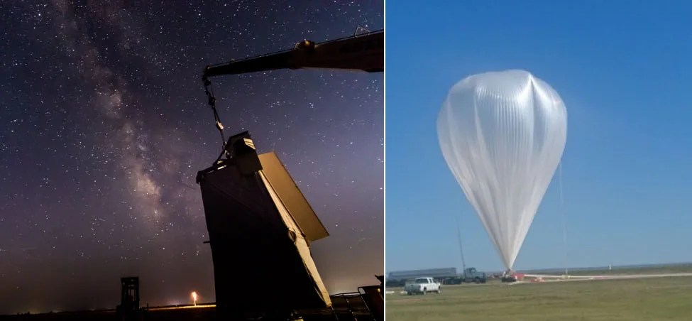
To prove this capability for future space missions, NASA is demonstrating 2D-doped and ALD-tailored detectors onboard the Faint Intergalactic Redshifted Emission Balloon’s follow-on mission, FIREBall-2 (FB-2). Although the first flight of FB-2 suffered premature loss of altitude due to a defective balloon, FB-2 successfully demonstrated all aspects of detector capability and detected some targets that a previous FIREBall mission did not. The technology will be further demonstrated in the next two FB-2 flights.
This ability to precisely engineer detectors’ surfaces and interfaces has created spinoffs into other areas. The same atomic-scale growth and deposition technologies have been extended to ultrathin protective coatings for UV/Optical mirrors, enabling the NASA JPL group to develop and deploy more compact and powerful cameras and spectrometers. These technologies’ advantages in performance, size, weight, and potentially power are applicable to a wide array of UV instruments, including an imaging spectrometer under development at the Principal Investigator’s laboratory at JPL. In addition, NASA’s newly selected Gravitational wave Ultraviolet Counterpart Imager has baselined these technologies to accomplish enhanced UV science using a small, compact instrument.
The research was carried out at the Jet Propulsion Laboratory, California Institute of Technology, under a contract with the National Aeronautics and Space Administration (80NM0018D0004).
PROJECT LEAD
Dr. Shouleh Nikzad, NASA Jet Propulsion Laboratory, California Institute of Technology
SPONSORING ORGANIZATION
Astrophysics Division‘s Cosmic Origins (COR) and Physics of the Cosmos (PCOS) Programs