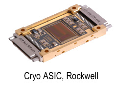
Light from faint astronomical objects is converted into faint electrical signals by the detectors in each of the James Webb Space Telescope's scientific instruments. These detector output signals are very susceptible to being overwhelmed by electrical noise. Just like AM radio or old pre-digital TV, analog signals are easily distorted and obscured by noise, but digital signals not so much. So converting analog signals to digital ones right near the detectors before sending them through wires to other processing and communications electronics away from the instruments is key to Webb science data integrity and quality, and consequently scientific measurement sensitivity.
Engineering Challenge
Such analog-to-digital or "A-to-D" conversion is nothing new, but the stressing technical challenge that Webb faced was doing it at the observatory's super-cold cryogenic operating temperatures in an Application-Specific Integrated Circuit (ASIC). The technology developed for Webb to do high-fidelity A-to-D signal conversion at cryogenic temperatures of faint signals from the detectors in its three near-infrared instruments is the SIDECARTM, or System Image, Digitizing, Enhancing, Controlling and Retrieving ASIC.
Each SIDECARTM ASIC 'chip' amplifies the voltage of the faint detector analog signal, converts it to a 16-bit digital signal, and organizes it into 'packets' before sending it to other processing and storage electronics on Webb so that after it is transmitted to Earth it can be 'reconstructed' into images and spectral information. SIDECARTM ASICs are programmable so their functions can be tailored to meet the needs of a particular science instrument or observation.
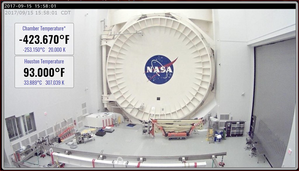
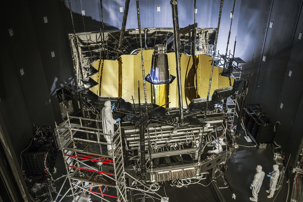
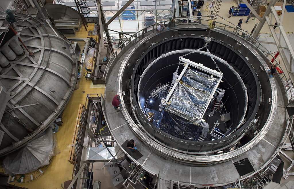
Webb operates at extremely cold temperatures in space, on the order of ~39K. The instruments and telescope optics were all put through their paces during testing to ensure that they would perform correctly in space.
